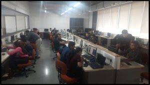
Department of Electronics and Communication Engineering, Institute of Technology, Nirma University organized a two-day National level workshop on “VLSI Chip Design using Cadence” during May 05 – 06, 2023. More than 35 students from UG, PG and Ph. D. participated in the said workshop.
The first day of the workshop was dedicated to custom IC design. In the beginning, Dr. Vijay Savani, introduced the various VSLI Design tools and their usage; both Dr. Savani and Dr. Akash Mecwan covered the entire custom IC design flow, starting from schematic to generation of GDS file.
On the second day, Dr. Piyush Bhatasna covered the entire ASIC design flow starting from Verilog coding to GDS file generation. In the second half students were introduced to cornet analysis, Monte Carlo analysis and process variations. The last session was dedicated to RF design simulations, where the case of LNA design was presented and the necessary simulations were carried out.
It was a fruitful learning experience for all the participants, they also practiced on the tool after the workshop hours in the lab.
The schedule of the workshop was as follows:
| 05-05-2023 | 06-05-2023 | |
| 9:00 to 10:00 | Introduction to the programme and Cadence Design Suite | ASIC Design Flow using Cadence |
| 10:0 to 11:00 | Design & Simulation using Cadence Virtuoso | |
| 11:15 to 12:15 | Design & Simulation using Cadence Virtuoso | RF Design and Simulation using Cadence Virtuoso |
| 12:15 to 1:15 | Layout Design and Simulation | |
| 2:00 to 3:00 | Layout Design and Simulation | Hands On Practice Session |
| 3:00 to 4:00 | Process Variation, Corner Analysis and Monte Carlo Simulations | |
| 4:15 to 6:15 | Hands On Practice Session |